Two recent software-based algorithmic technologies –– autonomous driving (ADAS/AD) and generative AI (GenAI) –– are keeping the semiconductor engineering community up at night.
While ADAS at Level 2 and Level 3 are on track, AD at Levels 4 and 5 are far from reality, causing a drop in venture capital enthusiasm and money. Today, GenAI gets the attention, and VCs eagerly invest billions of dollars.
Both technologies are based on modern, complex algorithms. The processing of their training and inference shares a few attributes, some critical, others important but not essential: See table I.

Source: VSORA
The remarkable software progress in these technologies has until now not been replicated by advancements in algorithmic hardware to accelerate their execution. For example, state-of-the-art algorithmic processors do not have the performance to answer ChatGPT-4 queries in one or two seconds at a cost of ¢2 per query, the benchmark established by Google search, or to process the massive data collected by the AD sensors in less than 20 milliseconds.
That is until French startup VSORA invested brainpower to address the memory bottleneck known as the memory wall.
The Memory Wall
The memory wall of the CPU was first described by Wulf and McKee in 1994. Ever since, memory accesses have become the bottleneck of computing performance. Advancements in processor performance have not been mirrored in memory access progress, driving processors to wait ever longer for data delivered by memories. At the end, processor efficiency drops way below 100% utilization.
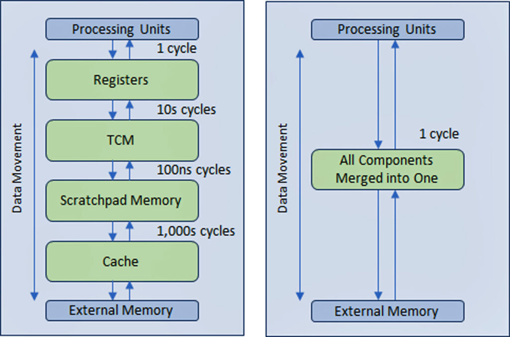
To solve the problem, the semiconductor industry created a multi-level hierarchical memory structure with multiple levels of cache nearer the processor that reduces the amount of traffic with the slower main and external memories.
Performance of AD and GenAI processors depends more than other types of computing devices on wide memory bandwidth.
VSORA, founded in 2015 to target 5G applications, invented a patented architecture that collapses the hierarchical memory structure into a large high bandwidth, tightly coupled memory (TCM) accessed in one clock cycle.
From the perspective of the processor cores, the TCM looks and acts like a sea of registers in the amount of MBytes versus kBytes of actual physical registers. The ability to access any memory cell in the TMC in one cycle yields high execution speed, low latency, and low-power consumption. It also requires less silicon area. Loading new data from external memory into the TCM while the current data is processed does not affect system throughput. Basically, the architecture allows for 80+% utilization of the processing units through its design. Still, there is a possibility to add cache and scratchpad memory if a system designer so wishes. See figure 1.

Through a register-like memory structure implemented in virtually all memories across all applications, the advantage of the VSORA memory approach cannot be overstated. Typically, cutting-edge GenAI processors deliver single digits percentage efficiency. For instance, a GenAI processor with nominal throughput of one Petaflops of nominal performance but less than 5% efficiency delivers usable performance of less than 50 Teraflops. Instead, the VSORA architecture achieves more than 10 times greater efficiency.
VSORA’s Algorithmic Accelerators
VSORA introduced two classes of algorithmic accelerators –– the Tyr family for AD applications and the Jotunn family for GenAI acceleration. Both deliver stellar throughput, minimal latency, low-power consumption in a small silicon footprint.
With nominal performance of up to three Petaflops, they boast a typical implementation efficiency of 50-80% regardless of algorithm type, and a peak power consumption of 30 Watts/Petaflops. These are stellar attributes, not reported by any competitive AI accelerator yet.
Tyr and Jotunn are fully programmable and integrate AI and DSP capabilities, albeit in different amounts, and support on-the-fly selection of arithmetic from 8-bit to 64-bit either integer or floating-point based. Their programmability accommodates a universe of algorithms, making them algorithm agnostic. Several different types of sparsity are also supported.
VSORA processors’ attributes propel them to forefront of the competitive algorithmic processing landscape.
VSORA Supporting Software
VSORA designed a unique compilation/validation platform tailored to its hardware architecture to ensure its complex, high-performance SoC devices have plenty of software support.
Meant to put the algorithmic designer in the cockpit, a range of hierarchical verification/validation levels –– ESL, hybrid, RTL and gate –– deliver push-button feedback to the algorithmic engineer in response to design space explorations. This helps him or her select the best compromise between performance, latency, power and area. Programming code written at a high level of abstraction can be mapped targeting different processing cores transparently to the user.
Interfacing between cores can be implemented within the same silicon, between chips on the same PCB or through an IP connection. Synchronization between cores is managed automatically at compilation time and does not require real-time software operations.
Roadblock to L4/L5 Autonomous Driving and Generative AI Inference at the Edge
A successful solution should also include in-field programmability. Algorithms evolve rapidly, driven by new ideas that obsolete overnight yesterday’s state of the art. The ability to upgrade an algorithm in the field is a noteworthy advantage.
While hyperscale companies have been assembling huge compute farms with multitudes of their highest performance processors to handle advanced software algorithms, the approach is only practical for training, not for inference at the edge.
Training is typically based on 32-bit or 64-bit floating-point arithmetic that generates large data volumes. It does not impose stringent latency and tolerates high-power consumption as well as substantial cost.
Inference at the edge is typically performed on 8-bit floating-point arithmetic that generates somewhat less amounts of data, but mandates uncompromising latency, low energy consumption, and low cost.
Impact of Energy Consumption on Latency and Efficiency
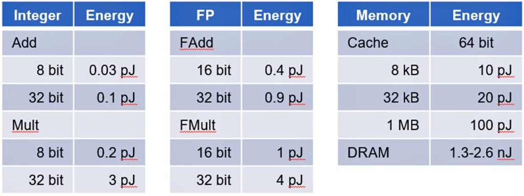
Power consumption in CMOS ICs is dominated by data movement not data processing.
A Stanford University study led by Professor Mark Horowitz showed that the power consumption of memory access consumes orders of magnitude more energy than basic digital logic computations. See table II.

AD and GenAI accelerators are prime examples of devices dominated by data movement posing a challenge to contain power consumption.
Conclusion
AD and GenAI inference pose non-trivial challenges to achieve successful implementations. VSORA can deliver a comprehensive hardware solution and supporting software to meet all critical requirements to handle AD L4/L5 and GenAI like GPT-4 acceleration at commercially viable costs.
More details about VSORA and its Tyr and Jotunn can be found at www.vsora.com.
About Lauro Rizzatti
Lauro Rizzatti is a business advisor to VSORA, an innovative startup offering silicon IP solutions and silicon chips, and a noted verification consultant and industry expert on hardware emulation. Previously, he held positions in management, product marketing, technical marketing and engineering.