The unstoppable rise in design sizes has been taxing heavily the EDA verification tools. Dynamic power estimation tools are one example.
Source: EE Times

Several incentives entice consumers to upgrade their mobile gadgets frequently. From more functionality and enhanced user experience, to a more attractive user interface to enliven usage, lighter weight, longer battery life, and the list does not stop here. All considered, it seems that long battery life tops the list, and longer battery life directly correlates to lower power consumption.
Power consumption in microelectronics has seen a constant drop since the invention of the planar integrated circuit by Noyce and Kilby five decades ago. The planar technology made it possible to scale (shrink) solid-state devices. The smaller the transistors, the more transistors in the same area, the faster they switch, the less energy they consume and the cooler the chips run (for the same number of transistors).

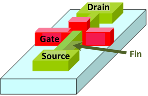
“Doublegate FinFET” by Irene Ringworm at the English language Wikipedia. Licensed under CC BY-SA 3.0 via Wikimedia Commons.
Historically, the metric for progress in microelectronics has been the length of the silicon channel between the source and drain terminals in field effect transistors, known as process technology node. At the beginning in 1960, the node was about 50µm. A decade later, it dropped below 1µm and, in 2003, below 100nm, starting the nanotechnology era.
For the first two decades, the static power consumption due to current leakage when the transistors do not switch and sit idle was smaller than the dynamic power consumed by transistors switching states, and small enough to be ignored. Then at 180nm, static power started to rise rather fast and, in 2005, as the node dropped below 65nm, it crossed over to dynamic power.
No worries. The invention of the FinFET or 3D transistor profoundly corrected the precipitous drive to extinction of the planar transistor.
FinFET is estimated to cut static leakage current by as much as 90%, and still use only 50% of the dynamic power of an equivalent planar transistor. Compared to the planar equivalent, FinFET transistors run faster, consuming the same amount of power, or run at about the same performance with less power. With FinFET, design teams can balance throughput, performance and power and meet the needs of each application.
The power estimation challenge
As stated earlier, lower process nodes lead to vastly more transistors for the same area presenting design teams with the opportunity to cram in more and more functionality. Today, the largest designs are exceeding 10-billion transistors. Unfortunately, this unstoppable rise in design sizes has been taxing heavily the EDA verification tools. Dynamic power estimation tools are one example. We can postulate that the dynamic power consumed by a circuit is proportional to the logic transitions that occur within the circuit when in operation. Therefore, for accurate power estimation and optimization of a digital circuit, we need to record the switching activity of each design element for each clock cycle, and feed that activity to the tool performing power-related tasks.
Recording the switching activity without keeping track of the corresponding cycle yields to average power consumption over the operational time window. By adding the cycle-by-cycle information permits to track peak power consumption.
It is intuitive to assume that the accuracy in recording the switching activity increases as the design description moves from the high level of abstraction down to the gate level and on to the transistor level, since more and more design details are available.
The dilemma is that at the electronic system level (ESL), designers experience the highest flexibility for comparing multiple architectures, various scenarios, or software algorithms and accomplish the best power optimizations. Unfortunately, at this level of description, power estimation is rather inaccurate. At the gate level and more so at the transistor level, where minuscule details are accessible, limited flexibility is available to accomplish anything other than marginal optimizations. It seems that at the register-transfer level (RTL), one can realize the best compromise. Enough details are accessible to achieve suitable estimates of power, and enough flexibility is available to reach sizeable power optimization.
Dynamic power consumption depends heavily on the activity within the design triggered by the stimulus applied to its primary inputs or, in the age of embedded SoC designs, by the embedded software executed by the embedded processors. That is to say, by booting an operating system, or executing drivers, applications or diagnostics.
Verification engines such as simulators and emulators are perfect vehicles to keep track of the switching activity. The caveat is the execution speed of simulators depends heavily on design level description, design size, and type of stimuli applied to the design. To alleviate and remove such dependencies, and to process embedded software, only emulators can perform the challenging task in a reasonable time frame.
Until now, the approach to estimate power consumption has been a two-step process. First, a simulator or an emulator tracks the switching activity cumulatively for the entire run in a switching activity interchange format (SAIF) file or on a cycle-by-cycle basis for each signal in a fast signal database (FSDB) file. Second, a power estimation tool fed with a SAIF file calculates the average power consumption of a whole circuit, or fed with an FSDB file computes the peak power in time and space of the design.
The above mechanism has two problems for SoC designs. SAIF and FSDB files are huge and almost unmanageable, and they require long time to be created. In the era of billion gates designs, the two issues combined are making this methodology useless.
Dr. Lauro Rizzatti is a verification consultant. He was formerly general manager of EVE-USA and its vice president of marketing before Synopsys’ acquisition of EVE. Previously, Lauro held positions in management, product marketing, technical marketing, and engineering. He can be reached at lauro@rizzatti.com