After dominating the computing landscape since the mid-1940s, the CPU architecture got demoted. As long as the escalating demand for powerful data processing outpaced the requirements for high bandwidth data movement, CPUs delivered what was expected from them. The rise of big data feeding high-performance computing (HPC) tilted the balance in favor of massive data movement throughput. A case in point is the elaboration of transformer algorithms in generative AI (GenAI) models that requires moving hundreds of billions of bytes every clock cycle, a daunting task that the CPU architecture cannot perform.
Never sitting idle, the semiconductor industry has been at work devising a multitude of alternative solutions, some more effective than others.
GPUs, FPGAs. and ASICs replaced CPUs in data centers and AI applications. However, while they boost data processing performance, none improves data movement throughput.
The culprit is the memory— specifically, inadequate memory bandwidth that has not kept up with the progress in data processing. The ensuant gap, which is known as the “memory wall,” hinders the efficiency of any processors. It also dramatically increases power consumption and thwarts their scalability.
The inherent potential of AI (specifically, GenAI) is severely incumbered by the limited bandwidth of memories. Although GPUs are the choice for AI learning in data centers, their efficiencies reportedly hover in a range of a single digit (that’s 1% to 9%)
One approach to address the memory wall, refined over the years, and still widely adopted, consists of buffering the memory channel in the proximity of the processor by inserting a multi-level hierarchical cache. By caching frequently used data, datapaths drastically shrink.

Moving down the hierarchy from the processors, the storage fabric changes from individual-bit addressable registers to tightly coupled memory (TCM), scratchpad memory, and cache memory. While storage capacity increases, speed of execution drops since more and more cycles are required to move data in and out of the memory
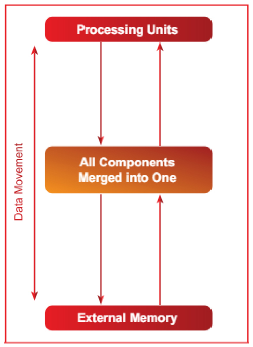
In an ideal scenario, replacing TCM, scratchpad, and cache with registers would lead to a massive speed up. That is what French startup VSORA did. The VSORA approach collapses the hierarchical memory structure into a large high bandwidth tightly coupled memory accessed in one clock cycle.
To the processor, the VSORA TCM looks and acts like a sea of registers in the amount of MBytes vs. kBytes in conventional computing architectures. The ability to access any memory cell in one clock cycle yields high execution speed, low latency, and low-power consumption. It also requires less silicon area. Loading new data from external memory into the TCM while the current data is processed does not affect system throughput.
This architecture allows for high utilization of the processors even when elaborating challenging applications. Typically, the efficiencies in executing large transformer models such as ChartGPT-4 on cutting-edge GenAI processors drop to single digits percentage. Instead, the VSORA approach on the same workload yields efficiencies in excess of 50%.
VSORA’s memory approach could reach two orders of magnitude higher processing efficiencies. That would lower the annual cost to run 100,000 queries per second— the standard established by Google search—on a GPT-4 system from hundreds of billions of dollars to fewer than $10 billion.