By switching to an emulation-based methodology, a company developing application processor units (APUs) can bring up the design on the emulator in days, and typical design changes can be accommodated in less than a day.
Source: Electronic Design

This year’s International Computer Electronics Show (CES) continued to amaze me with a never-ending display of mindboggling electronic gadgets. Choices encompassed a broad range of the latest generation of devices, from ultra-slim laptops to powerful tablets, amazing two-in-one mobile computers, and astonishing smartphones. Attention was paid to the now ubiquitous “Internet of Things” (IoT), simply defined as any device that communicates over the Internet and is not a computer. Among the IoT offerings, wearable devices, including smartwatches and health and fitness trackers, stood out as the new kids on the block of mobile devices.
Still, smartphones account for the largest share of the mobile market by a large margin, and no doubt are the drivers of the mobile market. At the core of such products sits an application processor unit (APU), the quintessential example of a system-on-a-chip (SoC) design.
The Application Processor
A little over a decade ago, Texas Instruments (TI) invented the terminology known as APU with its line of OMAP (Open Multi-media Applications Platform) devices. At the time, TI competed with Intel for what would be the next step in integration: Integration at the silicon level or integration at the package level, also known as system in package (or SiP). Intel claimed that chip-level manufacturing was a better fit for integrating different functions—memory versus digital processing versus analog circuits—by stacking individual integrated-circuit (IC) dies during the package assembly phase.
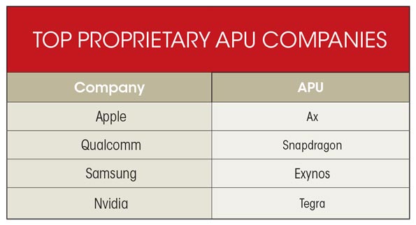
Unfortunately, after bringing five generations of OMAP devices to market, TI terminated the development of the OMAP family in 2012 because the market was excessively crowded. It was an acknowledgment of reality. Just consider that today all major semiconductor companies design their own flavor of AP. The table lists the major players in this competitive field.

On a single die, a typical APU integrates multiple ARM cores, several graphics processing units (GPUs), large on-chip cache memories, memory controllers for communicating with off-chip DRAM, audio and video decoders (and encoders), and USB host controllers. It also includes a plethora of other digital and analog circuit functions. Figure 1 represents a block diagram of a modern APU
An APU Case Study
A large mobile semiconductor company devised a modular application processor that supports the creation of a wide range of design sizes, from tens of million gates to hundreds of million gates.
Typically, the company provides its customer base with the AP and associated system software as part of development kits used to design next-generation mobile products. Kits give customers early access to working silicon and software. This enables them to get a jump on developing their own SoCs and embedded application software, and ultimately bring new products to market ahead of silicon and ahead of their competition.
To meet the pressure of this highly competitive marketplace, the company had to adopt new approaches to shrink its product development cycle. The most important was parallelizing its hardware- and software-development flows. It needed early prototypes of next-generation processors so that system software development teams could begin development of OS enhancements and drivers ahead of actual silicon. For this task, it selected a hardware emulation solution.
Like most developers of complex ICs, its engineers use register-transfer-level (RTL) simulation to verify intellectual-property (IP) blocks that make up the final AP design. However, performing integration-level testing at the full chip-level simulation is inefficient. With chip designs in excess of 100 million logic gates, chip-level simulation performance is less than one cycle per second—inadequate for booting the OS or running actual application software. Consequently, once the basic functionality of the chip is verified in simulation, the design moves into a hardware emulation platform to achieve runtime performance in the megahertz.
The emulation system was used by the chip-design team for processor verification, and by the software-development team for validating low-level system software. Once RTL code for the whole chip was available, the entire design moved to a high-capacity, high-performance emulation system with a maximum capacity of one billion gates for full system-level verification. The system-level prototype was shared among all software-development groups for local application development and validation.
This emulation system offered several benefits over traditional prototypes. For one, the entire design was contained within its hardware and associated PCs––it required no target board, avoiding external cabling, level shifters, and speed-adapters. As a replacement for a physical target system, the company relied on Mentor Graphics’ VirtuaLAB for each aspect of it, including cameras sensors, LCD display, external peripherals and multimedia interfaces. With this environment, the connection between the host and the emulator design was based on transaction-level interfaces.
The environment is a software implementation of in-circuit emulation (ICE) applications, where the design under test (DUT) is driven by the OS (e.g., Linux or Windows) using drivers, applications, and software stacks. This approach avoids the creation of hardware-verification testbenches (SysVerilog, for instance) not understood by software engineers. As a result, designers can create scenarios and environments well understood by software engineers.
Software tools, such as Mentor’s CodeLink, can be used for debugging in place of JTAG hardware (or even virtual JTAG) for non-intrusive debug. In a multi-processor environment found in APUs, whenever JTAG software debug is performed on one processor, that processor is halted and additional JTAG cycles are run, forcing it out of sync with other processors. Running simultaneous debug sessions only makes things worse, with more processors becoming out of sync. Because this type of software only traces data in a passive manner, emulation-based, multiprocessor software debug is a more robust option. The emulation system operates at megahertz speed, while exhibiting behavior that’s true to the final silicon.
In addition to making the system prototype inherently more reliable, the emulation system’s self-contained environment does not require human intervention to connect/disconnect external peripherals. The obvious benefit is that hardware- and software-development teams worldwide can share a single system at different times, 24/7, for different designs.
For example, the SoC hardware design team in one location uses it during the day for hardware verification. When everyone leaves for the evening, the team in another location can download a different design and use the same system for software development. In this way, the emulation system is kept running 24/7 without needing a local attendant.
Previously, the development team used a traditional field-programmable-gate-array (FPGA) prototyping system, and typically spent weeks trying to get the design to work correctly in the system. Such things as multi-FPGA partitioning, clock distribution, memory mapping, and bus handling required manual intervention.
When the inevitable design change would occur, the team often had to start the entire mapping process from scratch, incurring several more weeks of effort to get the modified design working correctly on the FPGA hardware. Once the prototype was working properly, the next hurdle was debugging. Internal visibility was limited and changing test points required major rework. As a result, it took a large team of engineers to support a single prototyping project.
Conclusion
By switching to an emulation-based methodology, a company developing APUs can bring up the design on the emulator in days, and typical design changes can be accommodated in less than a day. In addition, it can quickly debug problems with the emulation system’s interactive debugging environment. This can be accomplished with a combination of unique emulator hardware architecture-based custom silicon––Mentor Graphics, for instance, calls it “emulator-on-chip”––and the emulation system’s software that automates the mapping process and provides full, interactive design access for efficient debugging.
In the past, the goal was to deliver a stripped-down prototype system to software developers. Even then, projects were often a few months late. Now, the company shares a complete emulation system ahead of schedule. The real benefit, however, is that the company can ship higher-quality engineering samples to customers with a complete, validated software infrastructure. The financial impact of helping customers bring products to market sooner has been proven by several studies over the years.